MFOS Quad Timbre Bank
MFOS Quad Timbre Bank
product page: quad timbre bank
content courtesy of Ray Wilson
Features
Sample MP3sFilters modulated pulse input.
|  |
Introduction
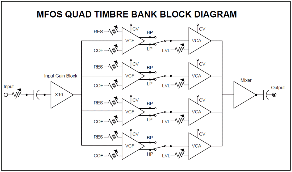
The MFOS Quad Timbre Bank began as a fixed filter bank but evolved into more. The board houses four 12dB/Oct resonant VCFs and four VCAs. Front panel controls for each VCF/VCA pair include cut-off frequency, resonance and output level. As shown here the board routes the input signal into four parallel VCF-VCA circuits. I liked the filter from the Echo Rockit so much that I used the design in this module. The exception is the filter capable of high-pass, lo-pass, and band pass. Another op amp was needed in that circuit to realize the highpass function. The low pass output is available from this filter as well on the PC board (at circuit point X37). In addition the cut-off frequency of each VCF and the output level of each VCA is able to be modulated independently with control voltage. The external CV modulation is linear in nature and not logarithmic so the filters are not intended to be 1V/Oct tone generators in sine oscillation mode.
Resonance can be increased to the point of oscillation. The level controls permit distortion at higher settings for unusual tonal generation. The cleanest sine waves are output when the BAND/LO-Pass filters are in low pass mode and in high pass mode for the fourth filter. In band pass mode all filter's output slightly distorted sine waves.
With some imagination the VCFs and VCAs can be routed in a variety of ways (independent, serial, par/ser) If I find myself with the time to experiment with this I'll document it here. In the mean time I hope benders and technologists out there give it a try.
The unit can be constructed without including the VCF and VCA control voltage input jacks if fixed filter bank functionality alone is desired.
The module draws 30mA from both the +12V and the -12V supply.
Schematics
Schematic Page 1
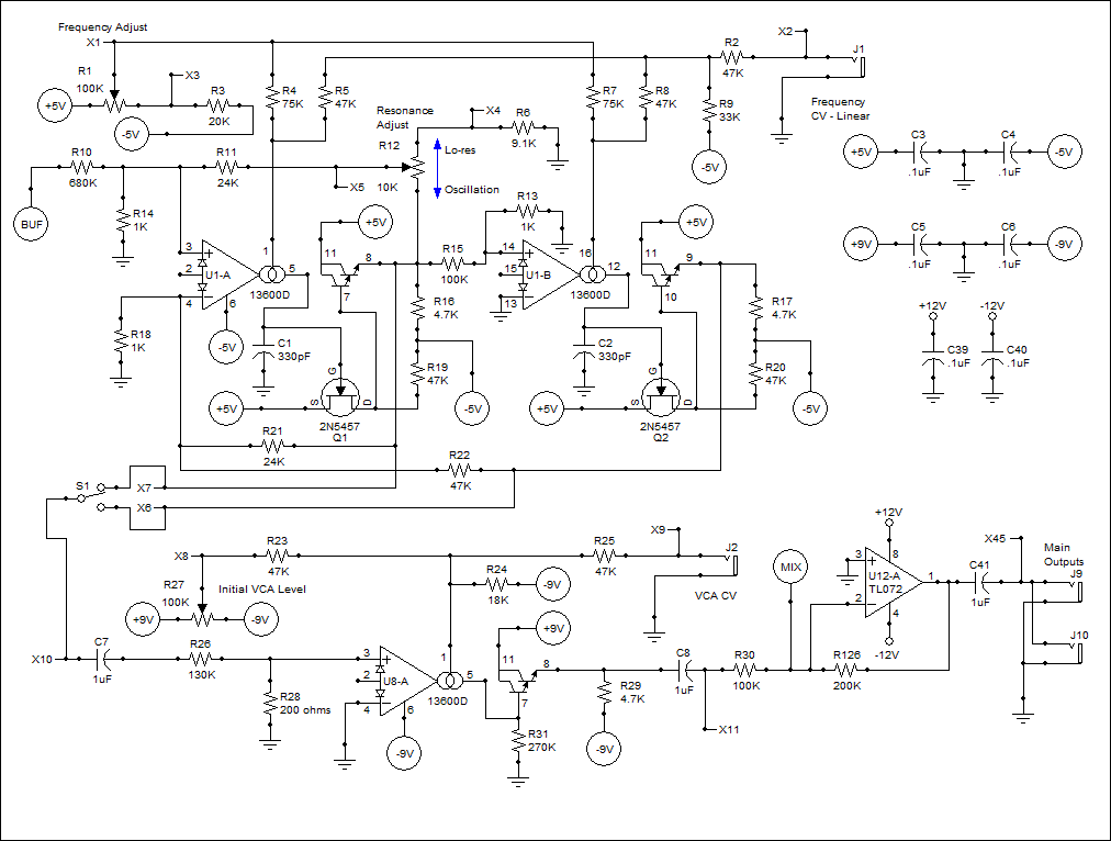
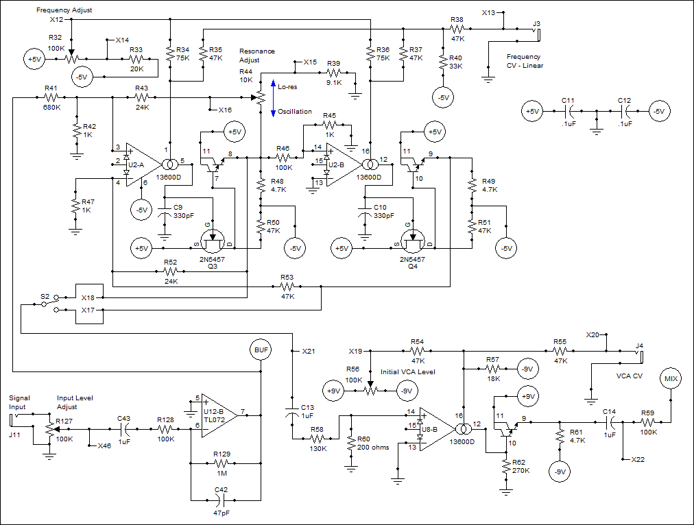
The VCF is the same design as used in the MFOS Echo Rockit and is powered by +/-5V provided by low power voltage regulators LM78L05 and LM79L05. Point BUF (output of the input buffer U12-B) is applied to attenuator network R10 (680K) and R14 (1K). The NJM13600D requires a very low level input signal to avoid overdriving its input. The NJM13600D dual transconductance op amp (and all subs) is used to provide us with linear voltage control. The VCF is a two pole low pass filter with voltage controllable poles. Current into U1 pins 1 and 16 controls the cut-off frequency of the filter. The resistive network comprised of R4, R7 and R9 in conjunction with the adjustable voltage from the wiper of R1 (100K linear pot) allow manual control of the filter's cut-off frequency. External control voltage can be applied to the tip terminal of J1 via resistors R2, R5, and R8 to externally control the filter's cut-off frequency.
The transconductance op amps in conjunction with their output capacitors (C1 and C2 both 330pF) act as voltage controlled integrators which form the filter's two poles. The integrated audio signals seen on C1 and C2 are buffered by high impedance source followers (Q1 and Q2 both N-Channel JFET 2N5457). The input impedance of the NJM13600D's onboard darlington pairs is too low and causes distortions and phase inaccuracies that prevent the filter from achieving oscillation. That is why we buffer the current output onto the filter caps with the high impedance gates of the N Channel JFETs (Q1 and Q2). The output of the JFET source followers is applied to the bases of the internal darlington pairs for buffering before driving additional circuitry.
The 10K resonance adjust control R12 ranges between no resonance and sine wave oscillation at the extreme ends of the knob's rotation. The low pass output of the filter (junction of U1-B pin 9 and 4.7K resistor R17) is applied to one of the poles of S1. The bandpass output (junction of U1-A pin 8 and 4.7K resistor R16) is applied to S1's other pole allowing either the band pass or the low pass output to be fed to the input of the VCA comprised of U8-A and associated components.
The signal presented to the VCA is attenuated by resistive network R26 and R28. Again the NJM13600D requires a low level signal to avoid distortion. Resistor R31 (270K) biases the output of the VCA to keep the output level within proper levels. The VCA's output U8-A pin 8 is dropped onto R29 4.7K resistor to -9V. The VCA is powered by +/-9V by means of using another pair of low power voltage regulators (LM78L09 & LM79L09). This allows the VCA to have a bit more headroom than the VCFs. Capacitor C8 (1uF aluminum bipolar) capacitively couples the VCA's output to the inverting output mixer (U12-A) via R30 which provides a gain of two due to R126 200K used as U12-A's feedback resistor. Output mixer U12-A's output is capacitively coupled to the output jacks (J9 and J10) wired in parallel.
Current into pin 1 of U8-A determines the level of the signal appearing at the output of the VCA U8-A pin 8. R27 delivers between -9V and +9V at its wiper which is used to bias the resistive network comprised of R23 (47K) and R24 (18K) to -9V. As the voltage is increased from -9V to +9V the VCA goes from fully off completely on (with slight overdrive). External CV via R25 can be used to linearly modulate the VCA's amplitude and will provide full modulation (off to fully on) when from -5V to +5V is applied and Initial Level is turned completely off.
Ceramic capacitors C3, C4, C5 and C6 (all .1uF) provide IC power supply bypassing for the low power regulator outputs. C39 and C40 (both .1uF) are used to bypass the board's incoming power supply in the vicinity of U12 which is powered with the full +/- supply entering the board.
The operation of the VCFs on schematic pages 2 and 3 are identical to the operartion of this VCF. The VCAs on pages 2, 3 and 4 operate in the same manner as this VCA. The designators are, of course, different.
Schematic Page 2
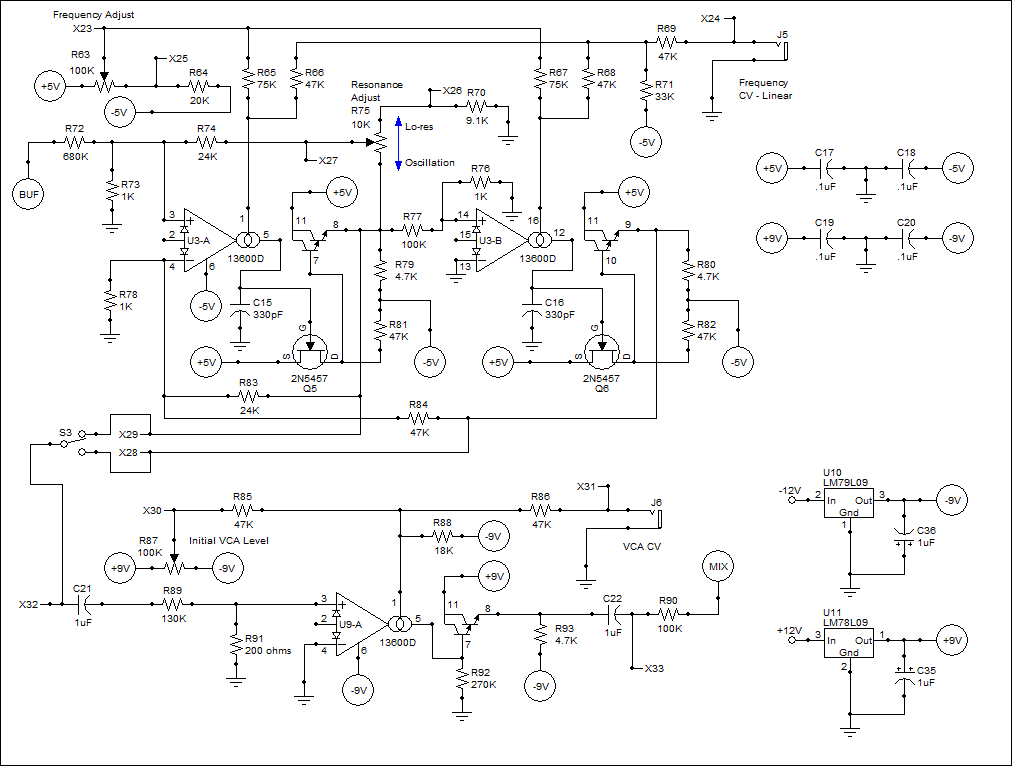
Page 2 shows the input buffer for the module (U12-B and associated components). The signal to be modified is applied to J11 which is wired across 100K linear Input Level Adjust pot R127. The wiper pf R127 is capacitively coupled to U12-B's 100K input resistor R128 which connects to U12-B's inverting input. The 1M feedback resistor R129 allows the input to be given a maximum gain of X10 when R127 is fully on. C42 stabilizes U12-B quelling any tendency to oscillate. The output of U12-B (point BUF) is applied to the input of all four of the modules VCFs. You can raise the maximum gain of the input buffer by reducing the value of R128 or increasing the value of R129. You can lower the maximum gain of the input buffer by increasing the value of R128 or reducing the value of R129. C11 and C12 are power supply bypass capacitors. Each IC has a pair near it's power pins on the PC board.
The VCF and VCA are identical in operation to that shown on Schematic Page 1.
Schematic Page 3
Page 3 contains another set of .1uF supply bypass capacitors (C17, C18, C19 and C20) for the low power voltage regulators. Additionally the +/-9V supply comprised of low power voltage regulators U11 (LM78L09) and U10 (LM79L09) respectively along with their 1uF tantalum output stabilizing caps are shown. These regulators supply power for the unit's four VCAs.
The VCF and VCA are identical in operation to that shown on Schematic Page 1.
Schematic Page 4
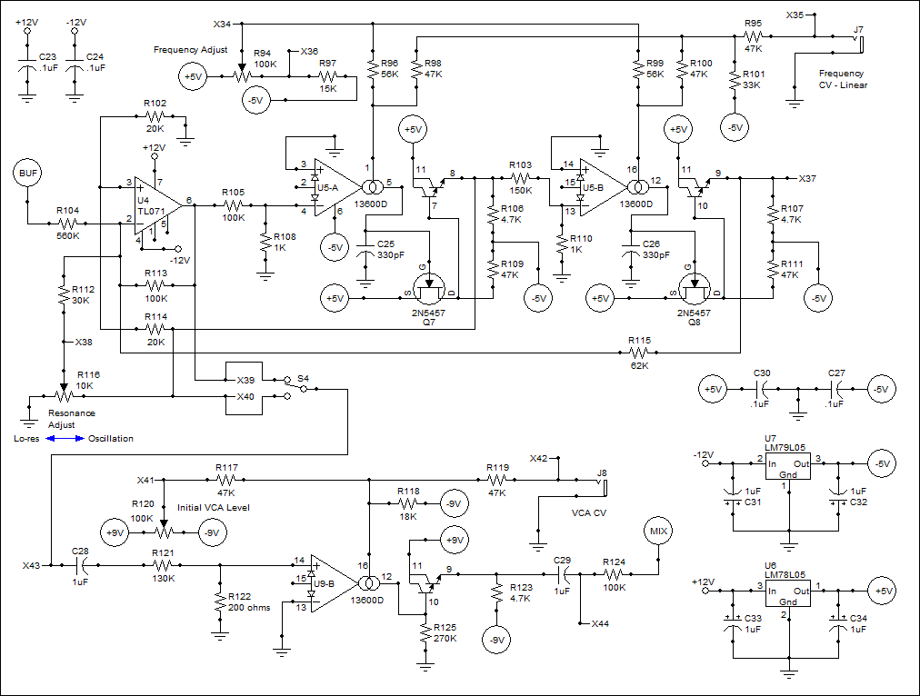
The VCF on this page is different from the previous ones in that an additional TL071 op-amp (U4) has been added to provide the differential summing necessary to realize the high-pass function of the state variable filter.
Feedback from the output of U5-B and the resonance control are applied to the inverting input of U4. The band pass output from U5-A is applied to the non-inverting input of U4. This combination causes the high pass function to be output from U4 pin 6.
Switch S4 permits application of this VCF's high pass or band pass output to the input of the VCA. The VCA functions in the same manner as the one shown on schematic page 1.
The unit's +/-5V supply comprised of low power voltage regulators LM78L05 and an LM79L05, which powers the module's four VCFs is also shown. Tantalum capacitors C31 and C33 stabilize the +/- power entering the board and serve both sets of voltage regulators (LM78L05/LM79L05 and LM78L09/LM79L09).
PC Board Information
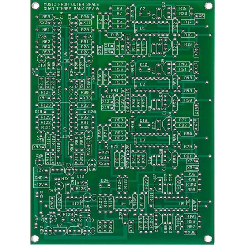
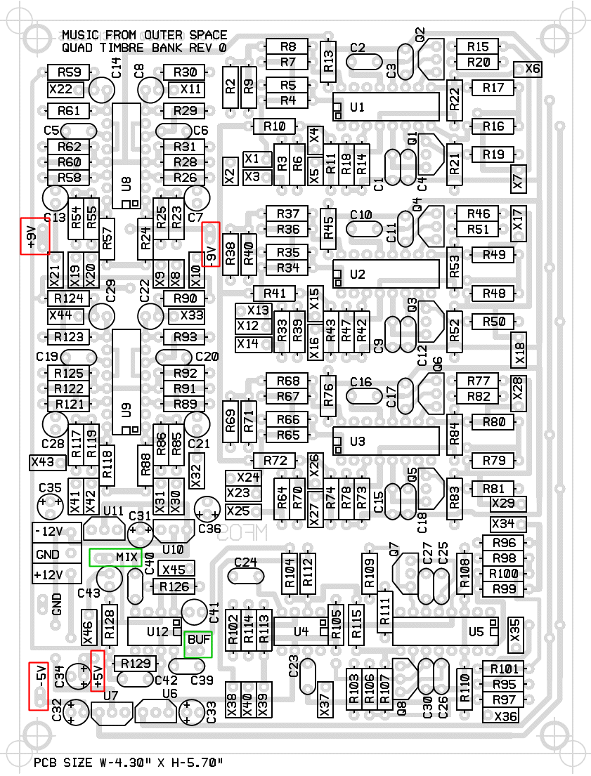
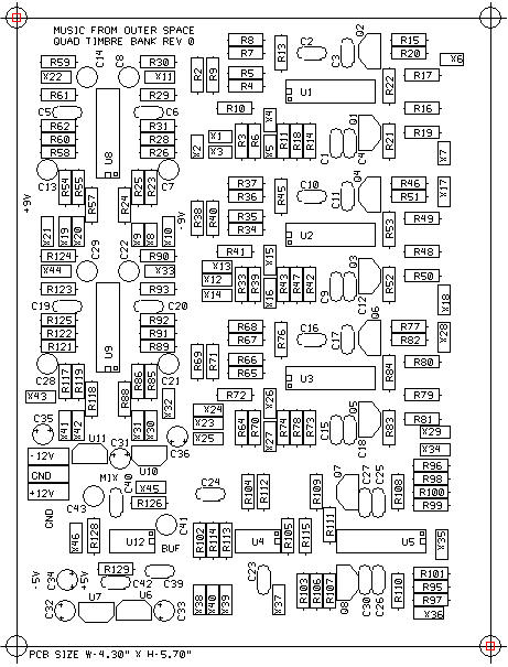
Parts Layout With Component Values
Use this view during board population so you don't have to keep referring back and forth from the schematic.
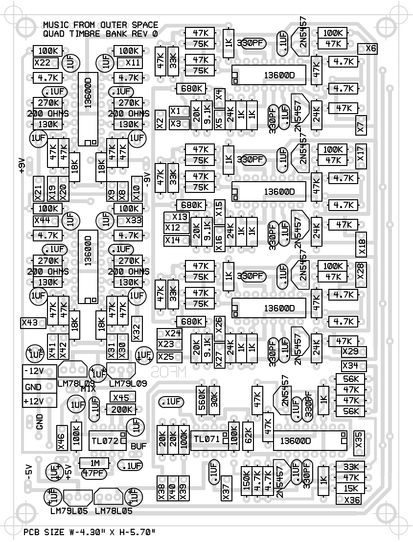
Parts Layout With Component Designators
Use this view during trouble shooting while referring to the schematic.
The red markers show the pads used for connecting the +/-9V and +5V to the front panel controls.
The green markers show the pads used for combining units for more filter channels.
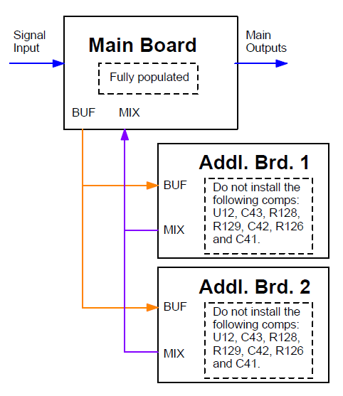
Adding More Channels - Combining Boards
You can use additional boards to increase the number of filter channels to 8 or even 12 if you like. To do this the main board is fully populated with components. The input signal is routed to it as shown in the wiring diagram. The main output also comes from the main board.
The additional boards used to provide more filter channels do not have the input buffer and output summer components installed because the main board provides both of those functions. The components to leave off of the additional boards are shown in the illustration below. The additional boards add more filter channels whose inputs are driven by the main board's buffered signal - point BUF. The outputs of the filters on the additional boards are fed into the main board's mixer - point MIX.
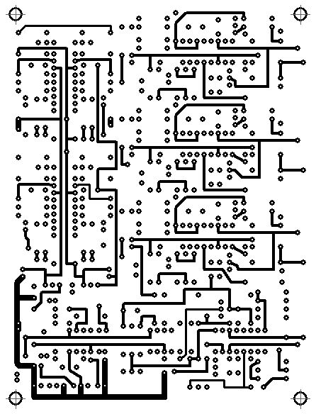
Top Copper
MFOS PCB Images are as viewed from the top of the PC Board. Keep that in mind when you are using the patterns with photo or copier processing. When printed out the pads should be 1/10 inch apart and 3/10 incha across. You'll need to futz with your image processing program's print scale.
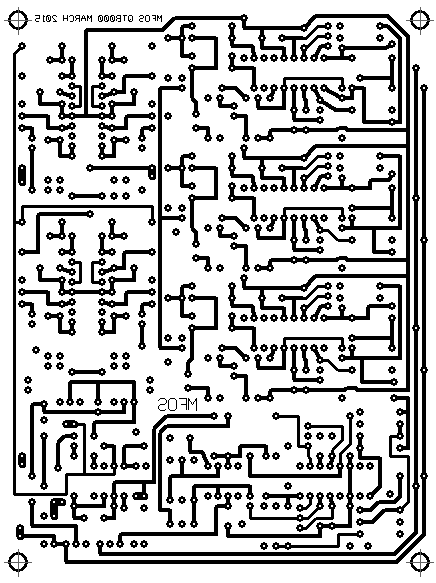
Bottom Copper
MFOS PCB Images are as viewed from the top of the PC Board. Keep that in mind when you are using the patterns with photo or copier processing. When printed out the pads should be 1/10 inch apart and 3/10 incha across. You'll need to futz with your image processing program's print scale.
Silk Screen
MFOS PCB Images are as viewed from the top of the PC Board. Keep that in mind when you are using the patterns with photo or copier processing.
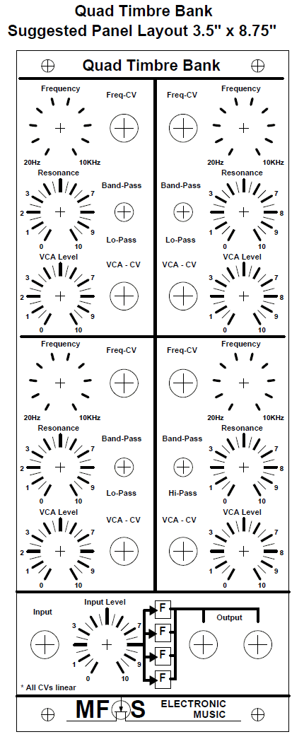
Front Panel Information
Suggested Front Panel Layout
The PDF image should be printed at actual size to obtain the 8.75" x 3.5" printout. Check your PDF programs print settings to ensure you get the correct dimensions.
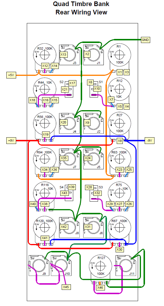
Suggested Front Panel Wiring Diagram
Note that the potentiometers must be the smaller sized ones (18mm instead of 24mm) in order for everything to fit onto the panel. I use the Amphenol ACJM-MV-2 1/4" jacks because of their smaller footprint for the same reason. I recommend 22 to 24 gauge stranded wire for the front panel intra-wiring as well as for connecting the panel components to the PC board's Xn circuit points.
Quad Timbre Bank Parts List
Component Notes
All cap voltages should be 25V or more. All resistors are 1/4W 5% (1% will work fine). MFOS PC boards use dual inline IC packages. MFOS PC boards usually use 5mm (0.2") cap lead spacing unless it is obvious from the board's legend that it should be larger or smaller. I often specify axial leads for any caps mounted on the front panel but you can use radial as well by adding some wire to the leads.
Note that 16mm pots and Amphenol ACJM-MV-2 are recommended if using the 3.5" x 8.75" panel.
| Qty. | Description | Value | Designators |
|---|---|---|---|
| 6 | 13600D Dual gm OpAmp | 13600D | U1, U2, U3, U5, U8, U9 |
| 1 | LM78L05 5V Voltage Regulator | LM78L05 | U6 |
| 1 | LM78L09 9V Voltage Regulator | LM78L09 | U11 |
| 1 | LM79L05 Voltage Regulator | LM79L05 | U7 |
| 1 | LM79L09 Voltage Regulator | LM79L09 | U10 |
| 1 | TL071 Op Amp | TL071 | U4 |
| 1 | TL072 Dual Op Amp | TL072 | U12 |
| 8 | 2N5457 N-Channel JFET | 2N5457 | Q1, Q2, Q3, Q4, Q5, Q6, Q7, Q8 |
| 9 | Potentiometer Linear taper 16mm | 100K | R1, R27, R32, R56, R63, R87, R94, R120, R127 |
| 4 | Potentiometer Linear taper 16mm | 10K | R12, R44, R75, R116 |
| 12 | Resistor 1/4 Watt 5% | 4.7K | R16, R17, R29, R48, R49, R61, R79, R80, R93, R106, R107, R123 |
| 6 | Resistor 1/4 Watt 5% | 75K | R4, R7, R34, R36, R65, R67 |
| 3 | Resistor 1/4 Watt 5% | 9.1K | R6, R39, R70 |
| 3 | Resistor 1/4 Watt 5% | 680K | R10, R41, R72 |
| 10 | Resistor 1/4 Watt 5% | 100K | R15, R30, R46, R59, R77, R90, R105, R113, R124, R128 |
| 4 | Resistor 1/4 Watt 5% | 130K | R26, R58, R89, R121 |
| 1 | Resistor 1/4 Watt 5% | 150K | R103 |
| 1 | Resistor 1/4 Watt 5% | 15K | R97 |
| 4 | Resistor 1/4 Watt 5% | 18K | R24, R57, R88, R118 |
| 11 | Resistor 1/4 Watt 5% | 1K | R13, R14, R18, R42, R45, R47, R73, R76, R78, R108, R110 |
| 1 | Resistor 1/4 Watt 5% | 1M | R129 |
| 4 | Resistor 1/4 Watt 5% | 200 ohms | R28, R60, R91, R122 |
| 1 | Resistor 1/4 Watt 5% | 200K | R126 |
| 5 | Resistor 1/4 Watt 5% | 20K | R3, R33, R64, R102, R114 |
| 6&a |