MFOS ECHOFXXX VC Echo Analog Synth Module
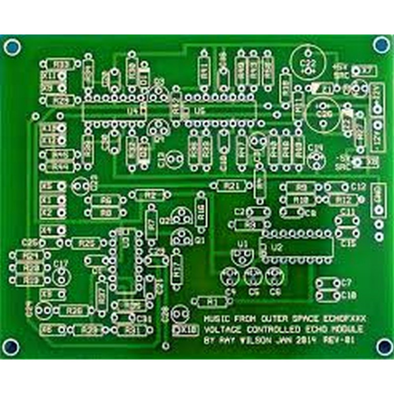
MFOS Voltage Controlled Echo Module Bare PCB
product page: mfos voltage controlled echo
content courtesy of ray wilson:
Features
Sample MP3sThese samples are all recorded using SONARbut no effects are added except for the ECHOFXXX Voltage Controlled Echo Module. Modulated Echo With Plinks
|  |
Introduction
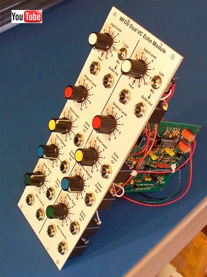
When I discovered the PT2399 Echo Processor IC I was certain I could use it to make a dynamite analog synth module. I have to say that the PT2399 did not let me down. Here is a photo of the dual unit I made requiring two PC boards. The PT2399 Echo Processor is total coolness on a chip. Lets take a look.
PT2399 Partial Block Diagram Explanation
Here we see a partial block diagram of the PT2399. See the Princeton Technologies PT2399 Data Sheet for complete details. The chip contains everything needed to generate echoes. While not specifically mentioned in the data sheet's text the data sheet's block diagram leads us to understand that the chip uses sigma delta modulation to achieve it's goal of audio signal delay.
In sigma delta modulation the input audio signal is converted to a one bit stream of logic levels which depend on the current direction (going high or going low) of the signal being converted. The clock rate is very high compared to the delayed audio signal's frequency in order to be able to use one bit sampling.
The chip also contains four op amps and a comparator which are used in the processing of the one bit data stream. All of the op amps share a common reference voltage (one half of the IC's supply voltage) which is applied to their non-inverting inputs. Analog signal levels through the chip are in the two volt peak to peak range while the chip's CMOS logic runs at the full 5V. The signal to be delayed is inserted into the chip (via a coupling cap and gain setting resistor) on pin 16. Low pass filtering is applied to the input signal to clean up any high frequency content that will not convert properly in the sigma delta circuitry that follows.
PT2399 Partial Block Diagram Princeton Technologies PT2399 Data Sheet

The output of the input conditioning low pass is applied to the inverting input of a comparator, the non-inverting input of which is connected to the output of the modulator being fed by DO0. My guess (again the data sheet is a little terse) is that DO0 (data out 0?) is the output of a one bit data latch into which the one bit converted audio data is stored until the next clock pulse. The output of this latch most likely feeds the 44K bit memory which follows. The voltage on the comparator's inverting input will be compared to the output of the modulator (after low pass filtering) and will either go high or low depending on the difference detected. The output of the comparator is serially streamed into and through the PT2399's 44K bit memory. The delay applied to the audio data is determined by the frequency of the unit's VCO which provides the clock source for the device's logic. Higher VCO frequency translates into a quicker trip through the memory (shorter echo delays) while lower VCO frequency results in longer delays.
After the delay of being shifted through the PT2399's 44K bit memory the one bit audio data (DO1 data out 1?) is converted into it's original audio form via the unit's demodulator. The demodulator's output is low pass filtered and becomes the delayed audio (echo) information. This is a fantastic idea for a chip and I love how it sounds, however I would have appreciated if the designers had included a simple way to daisy chain several chips for longer delays. You can, however, daisy chain as many of these synth modules as you'd like to get longer delays. The circuit gives the full range of the PT2399's advertised delays and also allows you to explore very low clock rates to get really long noisy delays and odd sounding effects. At low clock rates you will get the noisiest dirtiest echo signal you ever loved to hear. You can also play with the module's feedback and allow it to cascade until it achieves the classic motor-boating effect. I can say with certainty - you gonna love dis module mahn!
MFOS ECHOFXXX Voltage Controlled Echo Module Schematic
Here is the unit's schematic which I will describe in detail in the following paragraphs. When trouble-shooting this is where to come to learn what you should be seeing or hearing within the circuit. I always suggest reading the circuit's description before a purchase as it will help deepen your understanding of the operation of the module and ensure it meets your expectations.
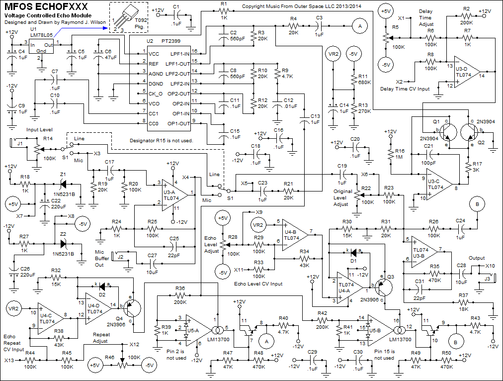
MFOS ECHOFXXX Circuit Description
We power the PT2399 chip (U2) with a LM78L05 IC which is a low power version of the popular LM7805 5V 1A regulator. The "L" version of the regulator only supplies 100mA but that's way more than the 15mA needed for our PT2399. We place 1uF tantalum capacitors on both the input (C4) and the output (C5) of U1 (the LM78L05) to stabilize it. The rest of the circuitry is powered by +/-12V (or +/-15V). We add the reference voltage stabilizer cap (C6, 47uF aluminum electrolytic cap) shown in the PT2399's data sheet. This voltage is used to bias the PT2399's on-board op amp non-inverting inputs so that a single 5V supply can be used with them.
We produce a nice stable source of plus and minus five volts to use for the Echo Level, Echo Repeat and Echo Time controls. We use two 5V zener diodes (Z1 and Z2 - 1N5231B 5.1V zeners) to generate the voltages. Z1 is biased with R18 1K resistor to +12V which causes it to zener resulting in +5V appearing at the cathode of Z1. C22 (220uF aluminum electrolytic) is used as a charge reservoir and +5V stabilizer. We generate the -5V using R27, 1K resistor, to -12V and Z2's cathode connected to ground. The -5V is generated at the junction of R27 and the anode of Z2. C26 (220uF aluminum electrolytic) is used as a charge reservoir and -5V stabilizer. These voltages are tied to the ends of the resistive elements of the Repeat Adjust (R46), Echo Level Adjust (R28) and the Delay Time Adjust (R5) 100K linear taper pots. Thus the wiper of each of these pots can deliver a continuous range of voltage between -5V and +5V as it is turned from off to fully on. While the unit is designed to respond over it's full range with control voltages of -5V to +5V higher synth control voltages can safely be applied.
We use .1uF ceramic caps for the caps that hang off of the PT2399's CC1 and CC0 pins (C7 and C10). The PT2399 data sheet shows .082uF for these but I found that .1uF worked perfectly. I also used .1uF for the filtering caps in both the modulator and demodulator op amp feedback networks instead of the .082uF caps shown in the IC's data sheet. Feel free to use the .082uF caps as I would bet it will increase the frequency response of the unit slightly but I experimented with subbing cap values as low as (.047uF) for them and did not hear (or see) a noticeable difference from using the .1uF caps.
We use the op amps on the chip to apply low pass filtering to the input signal (U2 pins 15 and 16 and C2, R3) and then again to apply low pass filtering to the echo output signal (U2 pins 13 and 14 and C8, R10). The output of the chip after the delay through the internal 44K bit memory appears at U2 pin 14 and is further low pass filtered by R9 and C12. Reducing the value of R9 or C12 will pass more high frequency from the echo signal but at lower clock rates you will hear more digital noise. Some people may prefer the additional high frequency content despite the noise at low clock rates.
In order to control the echo volume and the echo feedback (repeat) we use two identical VCA circuits built around the two halves of the amazing LM13700 (or any of its substitutes including NJM13600 which I sell). I'll only describe the operation of the VCA used to control the echo feedback (repeat). U4-C and U4-D are used as a voltage to current convertor to change the -5V to +5V control voltage into a control current to drive U5-A (1/2 LM13700 Dual Transconductance Amplifier). U4-C operates as an inverting control voltage summer with gain of -.43. The inputs to the control voltage summer are X13 (Echo Repeat Control Voltage Input) and X12 (R46 wiper providing -5V to +5V). The 100K input resistors (R44 and R45) and the 43K negative feedback resistor (R38) give us our desired inverting gain of .43. Thus the -5V to +5V control voltage range is converted to a range of +2.15V to -2.15V. We add a -2V offset to U4-C's output so that the output voltage ranges from about +150mV to -4.15V. This range is needed to operate the voltage to current convertor in the correct range. We do this by applying a -1.4V bias (VR2 - 'V Ref 2') to the non-inverting input of U4-C again bearing in mind that although the inverting input undergoes a gain of -.43 the non-inverting input will see a gain of 1.43. Thus to bias U4-C to have 150mV on it's output with a -5V input voltage we apply -1.4V to U4-C's non-inverting input (-1.4V x 1.43 = -2.00V offset) and voila U4-D's output ranges from about 150mV to about -4.15V which is exactly what we need. The -1.4V (VR2) is generated by applying the zener generated -5V to a resistor divider made up of R11 (680K) and R13 (270K). Thus -5V divided by 950K equals 5.2uA and 5.2uA times 270K equals -1.404V which is just what we needed. C14, 1uF electrolytic capacitor, stabilizes the divided voltage. The output of U4-C is applied to the non-inverting input of U4-D where it is converted to current by U4-D's feedback transistor Q4 and supplied to the bias input of U5-A. D2 clamps any positive output excursion of U4-D's output to about +600mV. When the control voltage applied to U4-C via R44 or R45 is low (-5V) the VCA is off (0uA of current flows into U5-A bias pin 1). As the voltage is increased towards +5V the VCA turns on more and more until it is fully on at +5V (approx. 290uA of current flows into U5-A bias pin 1). Thus the echo repeat feedback path can be controlled by a -5V to +5V control voltage applied to the Echo Repeat CV input or by the Echo Repeat knob on the front panel (which also supplies a -5V to +5V control voltage to U4-C).
The delayed echo signal from U2 pin 14 is applied, via C13 (1uF bipolar capacitor), to the non-inverting input of U5-A (1/2 LM13700 or equivalent) via 200K resistor R36. The inverting input of U5-A (pin 4) is connected to ground. The 1K resistor (R39) connecting the non-inverting input to ground attenuates the input signal by a factor of 200 to 1. We do this because the LM13700 only requires a few 10s of millivolts of input signal level to function properly. Applying as much as 50mV could result in severe distortion. Since we are shooting for 2V peak to peak signal levels through the PT2399 chip we end up applying about 20mV of signal after the attenuation to the non-inverting input of U5-A which is right where we want our signal level for low distortion without biasing U5-A's on-board linearizing diodes (see the LM13700 data sheet). We bias the base of the LM13700's on-board NPN darlington pair using R47 (47K to ground) and R48 (470K to +12V) so that the VCA's output seen at U5-A pin 8 oscillates nearly about ground and provides a gain of about one (at max control voltage) compared to the signal applied to the junction of C13, R36, and R42.
The output of this VCA (U4-C, U4-D, U5-A and associated components) appears at circuit point "A" which is connected to the PT2399's input (U2 pin 16) via C3 (1uF bipolar cap) and R4 (20K resistor). Thus echo recirculation can be voltage controlled.
The other VCA (U5-B and associated components) operates in a similar manner and allows the echo volume to be voltage controlled or controlled via the front panel's Echo Level potentiometer R28 (100K pot).
The input signal is connected to J1 (two conductor phone jack) where it is applied across 100K voltage dividing input level pot R14. The portion of the input signal picked off of R14's wiper is applied to one of the common poles of S1 (DPDT On-None-On switch). When S1 is in "Mic" position the input signal is applied to the non-inverting gain block comprised of U3-A and associated components. Resistor R19 (20K) insures that the input stays quiet when we are in "Line" input mode - disconnected from the input jack by switch S1. The signal dropped on R19 and coupled through C17 (1uF bipolar capacitor) is dropped onto R20 (100K resistor) and fed to the non-inverting input of U3-A. U3-A's 100K negative feedback resistor and its 1K resistor from the inverting input to ground apply a gain of 101 to signals passing through U3-A. C25 supresses any tendency U3-A may have to oscillate due to it's high gain. As a bonus U3-A's buffered signal appears at panel jack J2 (when "Mic" input is selected) for use with other synth modules that require an amplified audio signal. Use "Mic" input buffering for electric guitars, microphones, etc. and use "Line" input for higher level synth signals. With S1 in "Line" position the input signal bypasses the x100 gain block to avoid driving the amplifier into total saturation which would add noise to the system. If less gain is desired in "Mic" input mode then increase R24's value. For example: R24=1K then G=101, R24=2K then G=51, R24=3K then G=34.3, etc.
The common pole of S1 connected to PCB port X5 connects the input signal to the input of the echo processor chip via C23 (1uF bipolar capacitor) and R21 (20K resistor). The input signal sees a gain of 1 through the PT2399's op amp (pins 15 and 16) as we use a 20K negative feedback resistor (R3). The input signal should be adjusted via R14 so that there is between 1 and 2 Volts peak to peak observed at X5. Circuit point X5 also connects the input signal directly to the 100K linear taper Original Signal Level pot R22 which allows adjustment of how much original (non-echoed) signal appears at the output of the module's mixer/buffer U3-B.
Output buffer/mixer U3-B is used as a non-inverting mixer with gain of 27 so that the output is in phase with the input. The output of the VCA that is used to control the Echo Level (circuit point B) is applied to the non-inverting input of U3-B via 1uF bipolar AC coupling cap C24 and 100K mixing resistor R26. AC coupling cap C19 (1uF) capacitively couples the signal at circuit point X5 to the resistive element of Original Level Adjust 100K potentiometer R22. The portion of the Original Level signal picked off at the wiper of R22 is applied to U3-B's non-inverting input via 100K mixing resistor R23. U3-B's non-inverting input is biased to ground by 20K resistor R31. Since the input resistors to the output buffer are 100K we are attenuating the signals by dropping them on 20K R31 which is connected to ground. To compensate for this we add a gain of about 27 to the output mixer/buffer with 470K negative feedback resistor R35 and an 18K resistor R37 from U4-A's inverting input to ground. This is to boost the output levels up to synth level signals (approx +/-5V or better). If you need more output gain make R37 lower in value, less output gain make R37 higher in value. Remember gain formula for non-inverting op amp is (feedback resistor value divided by resistor to ground value) plus 1. With the values shown you will see a gain of 27 which given our 1V to 2V peak to peak internal levels will translate to 6V PP to 10V PP (+/-3V to +/-5V) of output level. The output of the module is capacitively coupled to the output jack (J3) via C28 10uF bipolar capacitor. The output levels are somewhat dependent on the input level seen at circuit point X5 which I recommend is in the 1 to 2 Vpp region. With the "Mic" (x100) input selected you will have no problem adding whatever gain you need to a low level signal.
Finally we get to the module's echo delay control. I basically took a linear voltage to exponential current convertor and tailored it to sink the current I needed to simulate the resistor to ground that the data sheet shows as the mechanism to adjust the clock frequency. I added a 1K resistor in front of the VCO control to insure that we stayed within the parameters of the PT2399 IC. The data sheet shows 1K as the lowest possible value for the VCO control (with a corresponding delay of 40mS). We convert the +/-5V control signal into a current sink that causes the VCO frequency to be low when the control voltage is low (small current being sinked simulates high value resistor for clock timing resistor R) and high when the control voltage is high (larger current being sinked simulates low value resistor for clock timing resistor R). See the PT2399 data sheet for explanation of the "R" I'm referring to.
There are several bypass capacitors strewn around the schematic (caps connnected to +V or -V and ground). A pair of .1uF capacitors decouples each IC except U2 (which is decoupled by C5).
The module is a little current hungry and draws about 47mA from the positive 12V supply and about 27mA from the negative 12V supply. We are using more current from the positive rail to run the LM78L05 regulator and the PT2399 chip.
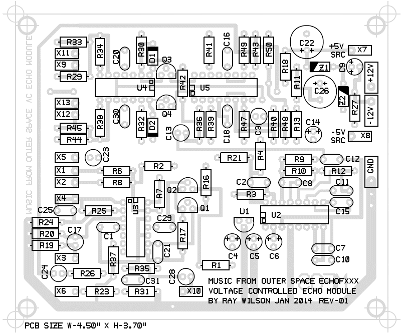
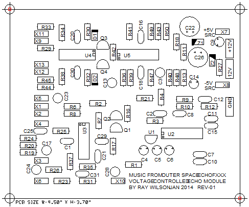
PC Board Designator View
Use this view during trouble shooting to find components shown in the schematic.
PC Board Designator View
PC Board Value View
Use this view during board population so you don't have to keep referring back and forth from the schematic.
PC Board Value View

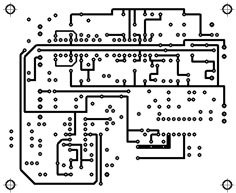
PC Board Top Copper
Top copper. All layers are as viewed from the top side of the PC board.
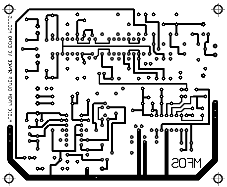
PC Board Bottom Copper
Bottom copper. All layers are as viewed from the top side of the PC board.
PC Board Silk Screen
Designators silk screen. All layers are as viewed from the top side of the PC board.
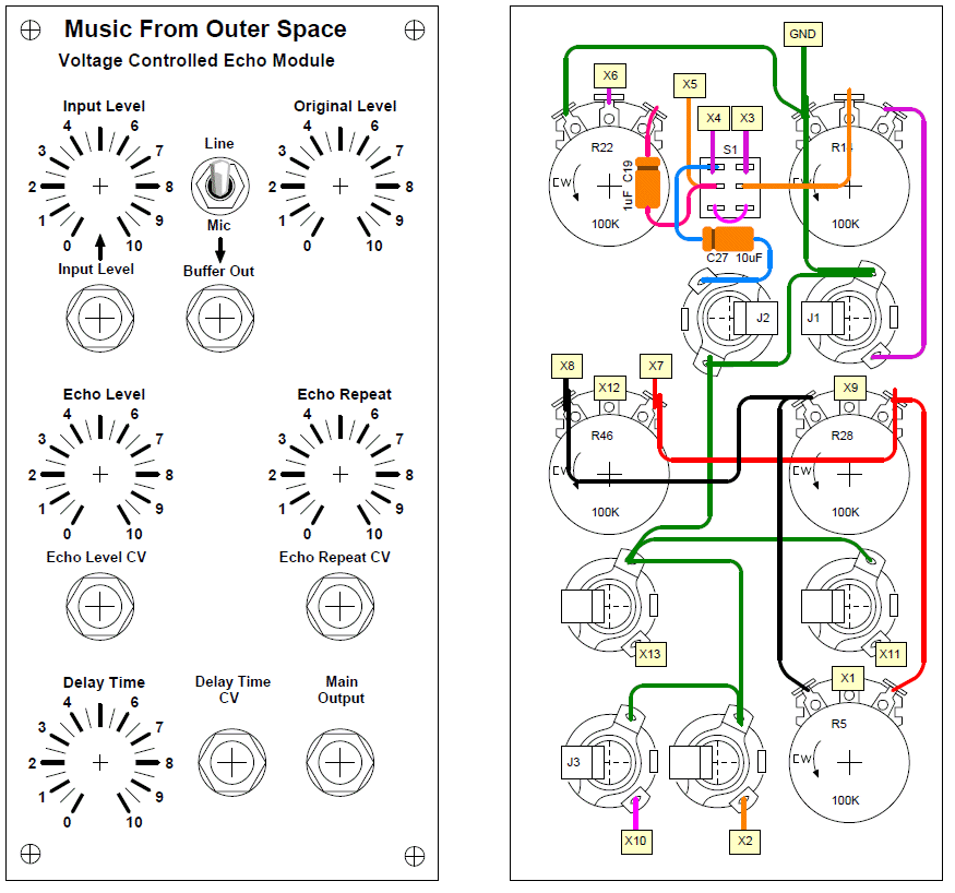
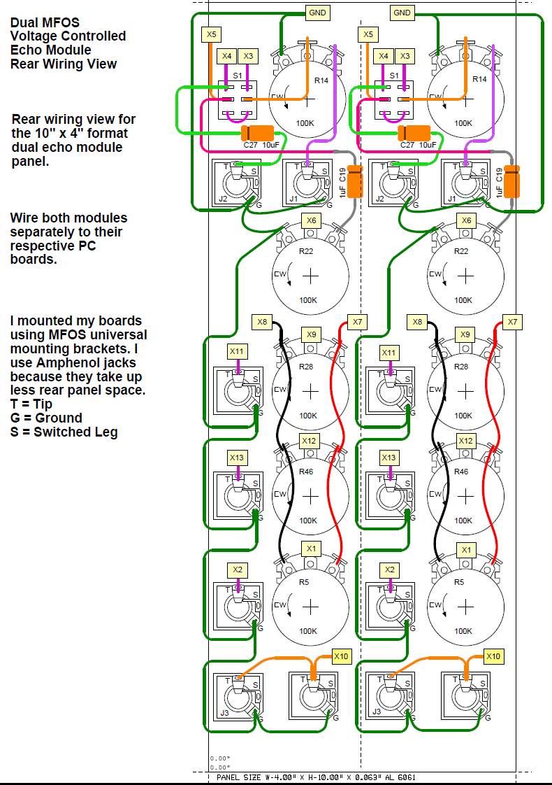
Panel Template and Wiring View
This panel is for demonstrating the connections from the PC board to the front panel. I'm sure your imagination can do better than this - however this definitely works in a pinch. Capacitors C19 and C27 are mounted on the front control panel.
Panel Template and Wiring View
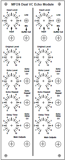
Four by Ten Dual Unit Panel Template and Wiring View
This panel layout accomodates two units in a four by ten inch panel. They are wired as two separate units on the panel. I simply connected the output to two jacks because it should be able to drive two inputs easily.
Dual Echo Unit Panel Template (Click image for PDF)
Dual Echo Unit Panel Wiring (Click image for PDF)
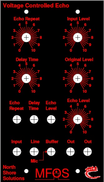
Mark Nordstrand shared this cool Frac-Rack version panel. It should be printed as 3" x 5.25". There is no wiring diagram for this plate. I suggest you create one if you use this design.
MFOS ECHOFXXX Voltage Controlled Echo Module Parts List
Component Notes
All cap voltages should be 25V or more. Caps with 0.2" (5mm) radial (as opposed to axial) style leads are the norm unless the board spacing requires otherwise (look at the board layout). All resistors are 1/4W 5% (1% will work fine). MFOS PC boards use dual inline IC packages.
Important
Designator R15 is not used.
Capacitors C27 and C19 (both 1uF Bipolar) are mounted on the front panel. Capacitors with axial leads are shown in the panel wiring diagram but caps with radial leads will work just fine too. I just added some extra wire to the leads of some radials for mine.
| Qty. | Description | Value | Designators |
|---|---|---|---|
| 1 | LM13700 (NJM13600) Dual gm OpAmp | LM13700 | U5 |
| 1 | LM78L05 5V Voltage Regulator (T092) | LM78L05 | U1 |


PT2399 Echo Processor Chip
PT2399 Echo Processor Chip view project SALE OF THIS ITEM IS FIN..
$6.50 Ex Tax: $6.50